SSTE32882KB1AKG8 – Low Power DDR3 Register + PLL

The SSTE32882KB1AKG8 is a low-power registering clock driver with integrated PLL, designed for DDR3 RDIMM (Registered Dual In-Line Memory Module) applications. It buffers one differential clock input and distributes it to multiple differential outputs.

Product Brochure

Description

Technical Specifications:

  • Type: Registering Clock Driver + PLL
  • Memory Type: DDR3 RDIMM
  • PLL: Yes
  • Input Type: LVCMOS (CK, CK#, RESET, MIRROR)
  • Output Type: LVCMOS (Clock outputs, Register outputs), Open-drain (ERROUT)
  • Number of Outputs: 1 (Register), 4 (Clock Pairs)
  • Ratio – Input:Output: 2:5
  • Differential – Input:Output: Yes/Yes
  • Frequency – Max: 810 MHz
  • Voltage – Supply: 1.282V to 1.575V
  • Operating Temperature: 0°C to 70°C
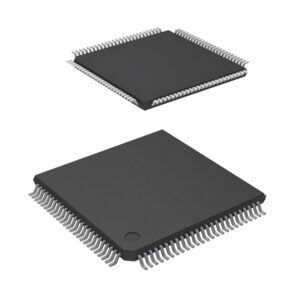
  • Package Type: 176-CABGA (8×13.5)

Product Features:

  • DDR3 Support: Compatible with DDR3-800/1066/1333/1600/1866/2133 data rates.
  • Register and Clock Outputs: Provides 1-to-2 register outputs and 1-to-4 clock pair outputs, supporting stacked DDR3 RDIMMs.
  • Integrated PLL: Features a Phase Lock Loop for low-jitter clock distribution.
  • Differential Clock Buffering: Buffers one differential clock pair (CK, CK#) and distributes it to four differential outputs.
  • LVCMOS Inputs: Supports LVCMOS switching levels on RESET and MIRROR inputs.
  • Parity Checking: Checks parity on DIMM-independent data inputs.
  • Dynamic Timing: Supports dynamic 1T/3T timing transactions and output inversion for improved performance.
  • Power Down Modes: Supports CKE Power Down operation modes for energy efficiency.
  • Quad Chip Select: Supports Quad Chip Select operation features.
  • RESET Functionality: Disables input receivers, resets registers, and disables output drivers (except ERROUT and QnCKEn) upon RESET.
  • Configurable Features: Provides access to internal control words for device configuration.

Reviews

There are no reviews yet.

Be the first to review “SSTE32882KB1AKG8 – Low Power DDR3 Register + PLL”

Your email address will not be published. Required fields are marked *

× Let's Talk